
Lightmatter
Top 100
Funding
Raised a $400M round on Oct 16, 2024, bringing the total raised amount to $850M.
Returns Calculator
A $10,000 investment at Series C-2 round (2023) would today be worth:
$36,667
3.7×the original amount
Illustrative · based on reported post-money valuations
Top posts
Serenity
@aleabitoreddit
I personally think $SIVE can be the next $LITE. In the past few months alone, we've seen: 1. Partnerships with O-Net pushing ELS into mass production 2. $JBL 1.6T LRO mass production signals with "relatively dramatic moats" for pluggables using Sivers. 3. $GFS SCALE reference level laser for hyperscalers with pluggable, NPO, CPO. -> -> where $AMD and others went to GFS for CPO. 4. Ayar, which joined $NVDA NVLink for CPO -> -> which removed Lumentum/Macom from their website and likely made Sivers their primary laser supplier. -> -> AlChip likely Trainium win from Amazon price placement (Ayar's customer) -> -> GUC rack level design in with Ayar. -> -> Raised $500m for mass production by AMD, Alchip, Mediatek, and NVIDIA 5. ~ $AEVA starting HVM H2 2026. 6. $POET starting HVM H2 2026 with hyperscaler suppliers like Lumilens ("top 3 hyperscaler initial customer") 7. TFLN + $SIVE CW Lasers with Lightium 8. Likely direct relationships with $MRVL Celestial and CPO players like Lightelligence/Lightmatter. 9. Multiple new undisclosed relationships for pluggables following Jabil in their quarterly transcripts With new Trendforce reports that $AMD and other hyperscalers are trying to source LTAs for CW laser sources, serving as a direct catalyst for independent CW sources. So when hyperscaler suppliers from Jabil to O-Net are incentivized to mass produce as many as they can: That's very material for revenue for Sivers relative to current valuations, and it looks like just a waiting game. Even in the past week: - $SIVE raised an oversubscribed institutional round for volume ramp... This is very nuanced since Sivers is fab-lite so it's not going to in-house foundry capex to scale. Likely toward Win Semi and others (they mentioned other partners too), for laser scaling + foundry allocations. So this is likely signaling material for revenue ramp is coming. - Sivers also mentioned NASDAQ listing completion targeted in the next few quarters (probably H2 2026 or Q1 2027 is my est. timeframe). This would fund M&A efforts, since it's impossible with the fundraising environments in local Swedish markets. As for becoming the next $LITE: M&A makes their lasers more valuable, so downstream IP acqusition -> into contract manufacturing like $FN, and others to make the full 1.6T pluggable or optical engines. Is how they get there, since laser array ASP scaling that people are modeling off of, wouldn't command a $60B+ valuations. There's going to be a lot of bridge architectures like NPO/pluggables, etc and noise around certain architectural delays in the meantime. But markets misunderstand laser companies like $LITE, $SIVE, $AAOI and others are used across different architectures compared to if you just look at certain passive optical components. So markets see "CPO delay headlines" algos sell off laser companies that benefit from other architectures. Being included in the pluggable 1.6T ramp to CPO scale out (Which Sivers is included in), helps bridge revenue waiting gaps until scale up inflection point H2 2027. I'm personally holding long term, since I haven't seen a ~$1.4B company mapping to this many hyperscalers before. TLDR: - Waiting on volume ramps from different architectures to play out across their hyperscaler supplier mapping -> 1.6T LRO/CPO scale out late H2 2026 start into high volume ramp 2027 -> H2 2027 CPO scale up volume ramp - Waiting on NASDAQ listing likely H2 2026/Q1 2027 for M&A efforts to fully take off, unless Sivers get more creative with equity financing in the meantime.
Trade Whisperer
@TradexWhisperer
Lightmatter Joins $TSM on COUPE Advanced Packaging Platform for 3D Optical Engines AI training clusters are hitting hard physical limits with copper interconnects. The shift to 1.6T (and beyond) optical bandwidth is turning silicon photonics (SiPh) and specialized lasers into critical bottlenecks. Lightmatter, a leader in photonic interconnects, is deepening its collaboration with TSMC using the foundry's COUPE (Compact Universal Photonic Engine) platform to commercialize 3D-stacked optical engines. This move leverages Taiwan's ecosystem to bridge photonics prototypes to high-volume production, positioning TSMC as a central player against competitors like Samsung TSMC's COUPE is a heterogeneous integration technology for silicon photonics in high-performance computing (HPC). It supports flexible 2D/2.5D/3D structures with low-loss coupling (grating or edge couplers), robust packaging without mechanical weaknesses, and seamless co-packaging with host ASICs. Broader ecosystem: Involves players like ASE, Amkor, and laser suppliers $ASX $AMKR Market implications: Faster commercialization of CPO/SiPh could unlock larger AI clusters, reduce power costs, and create new opportunities in optical components, packaging, and test. This development underscores photonics as the next high-growth layer in AI infrastructure—beyond logic and memory. Watch for: -Volume ramps in 2027+. -Laser/InP supply chain expansions. -Adoption by major hyperscalers and GPU/ASIC vendors. TSMC is just everywhere. ASICs, CPU, GPU/HBM, Optics. All In.
Unclestocknotes
@Unclestocknotes
Strong technical observations, weak market conclusion. Let me separate the two. What the post gets right:CoWoS does face real reticle-limit and thermal challenges as packages scale beyond 5.5x. EMIB's localized silicon-bridge architecture genuinely offers yield advantages in certain configurations. Intel has been investing in silicon photonics for ~25 years and has demonstrated impressive Optical I/O chiplet performance (2 Tbps @ ~5 pJ/bit). These are all defensible points. What the post gets wrong: The thesis rests on the premise that "TSMC has fumbled CPO." This is empirically false. CPO is already in volume production — just not from Intel. 1. Broadcom shipped more than 50,000 Tomahawk 5-Bailly CPO switches in 2025 — the industry's first volume CPO platform, built on TSMC. 2. Meta's published reliability study covers over 1 million 400G port-device-hours on Bailly with zero link failures. 3. Broadcom's third-gen Davisson (102.4 Tbps, 200G/lane) launched in October 2025 with TSMC's COUPE process as the foundry technology. 4. NVIDIA Quantum-X Photonics is GA in early 2026, with Spectrum-X CPO following in 2H26. TSMC COUPE enters volume production in 2026; CoPoS pilot line completes June 2026. Intel's 2024 Optical I/O demonstration remains exactly that — a demonstration. There is no customer shipment. On the 90% market share claim: The CPO market is structurally an ecosystem, not a single-vendor play. The supply chain includes ASIC vendors (Broadcom, NVIDIA, Marvell), foundries (TSMC, Tower, GlobalFoundries), laser and optical component suppliers (Coherent, Lumentum, Sumitomo), OSATs (ASE, SPIL, Amkor), and emerging silicon photonics specialists (Ayar Labs, Celestial AI, Lightmatter). Intel currently holds ~21.5% of the broader silicon photonics market- predominantly in pluggable transceivers, not CPO. For Intel to capture >90% of CPO within five years would require simultaneous failure across this entire ecosystem, combined with flawless execution from a company currently posting foundry losses, leadership transitions, and constrained capital. The probability is, charitably, in the low single digits. A more defensible framing: Intel as a 15–25% CPO player is a legitimate and interesting thesis. It would represent meaningful re-rating from current expectations and is supported by real architectural advantages in EMIB. But that case must be made on Intel's own merits, not by dismissing the fact that the TSMC + Broadcom ecosystem has already crossed the volume-production threshold while Intel has not. Technical superiority does not automatically translate into market share. The history of semiconductors is full of better architectures that lost — Itanium being the most famous example from Intel's own history. The CPO race is being decided in production racks today, not in 2030 forecasts. Good engineering reasoning. The market structure analysis needs more rigor.
Photon Capital
@PhotonCap
Optical networking is already widely used for scale-out connections across data centers, while low-latency scale-up links between GPUs inside a rack still rely primarily on copper technologies such as NVIDIA NVLink. As signaling speeds increase, copper links face greater attenuation, power consumption, and heat. NVIDIA plans to expand its tightly connected systems from 72 GPUs today to as many as 576 by 2027, and the company acknowledges that in-rack copper is approaching its physical limits. NVIDIA’s NVLink Fusion ecosystem now includes photonics companies such as Ayar Labs, Marvell, and Lightmatter. Ayar Labs is developing optical chiplets positioned beside processors, while Lightmatter is pursuing photonic interposers that can sit underneath compute chips. Improvements in foundry processes, hybrid bonding, packaging, and testing have made co-packaged optics more manufacturable. However, integrating large numbers of lasers efficiently and reliably remains a major challenge. NVIDIA is taking a gradual approach, adopting optics first in scale-out networks and potentially extending it into scale-up systems as bandwidth requirements increase. Industry participants expect multiple high-volume optical scale-up implementations around 2028, although this remains a forecast and copper is likely to coexist with optics for some time. --> Optical scale-up is being pursued through a wide range of architectures by multiple companies and engineering teams. Ayar Labs is developing optical chiplets, while Lightmatter is taking a photonic-interposer approach, and other implementations will continue to emerge. At this stage, predicting the eventual architectural winner is difficult. A more useful strategy is to focus on the common bottlenecks and chokepoints that every solution must pass through. As I have consistently argued, the two most critical layers in silicon photonics and co-packaged optics are packaging and measurement/testing. Optical devices, electronic chips, lasers, and fibers must be integrated with low loss, high yield, and sufficient reliability. Once assembled, both individual components and complete optical engines must also be tested at production speed and scale. As competition between architectures intensifies, these two layers are likely to determine which technologies can actually reach high-volume manufacturing.
Pep Invest
@PepInvestStocks
Lightmatter recently demonstrated the world’s first bidirectional 16-wavelength optical link over a single fiber. To build this ultra-fast connection for AI supercomputers, @LightmatterCo needs a physical laser source that can emit exactly 16 different wavelengths of light simultaneously, with extreme precision and stability. However, Lightmatter does not manufacture these lasers themselves. $SIVE is currently the only commercial laser manufacturer in the world that has officially developed, publicly validated, and delivered 16-wavelength Distributed Feedback (DFB) laser arrays in mass production. They originally developed this specific technology for their partnership with @AyarLabs . Because $SIVE is the only company offering this rare 16-wavelength laser technology, and Lightmatter is the only company building a 16-wavelength optical chip network, the industry conclusion is clear: Lightmatter must be using $SIVE technology.
revoAIution
@revoAIution
Dug into every possible optical linkage for $SIVE and MI500 after AMD's own executive confirmed optics will be used. MI500 launches 2027, and AMD confirmed it uses both copper and optical connectivity. Here's is what I found from most to least likely. Most likely = $GFS. TechPowerUp reported back in April that AMD is returning to $GFS specifically for CPO manufacturing on MI500 by name. $GFS's own SCALE deck lists AMD as an OCI MSA founding member alongside $AVGO, $NVDA, Meta, Microsoft, and OpenAI. The official June 2 $SIVE and $GFS press release confirms $SIVE laser arrays are integrated into reference designs on $GFS's silicon photonics platform, available in the SCALE platform for CPO and linear pluggable optics. No other laser company is named anywhere in that official announcement. Second = Ayar Labs. AMD directly invested in Ayar Labs' Series E funding round. Ayar Labs joined Nvidia's NVLink Fusion ecosystem in June and already demonstrated a full CPO scale-up rack with Wiwynn at OFC in March. $SIVE has been Ayar Labs' confirmed laser supplier since 2022. No confirmation this specific relationship is tied to MI500 by name yet though. Least likely, Lightmatter. Also joined NVLink Fusion, making them a direct competitor to Ayar Labs in that same ecosystem slot. One unverified source claims AMD backing here too. This wouldn't touch $SIVE at all, so would be the worst outcome. Lightmatter builds its own proprietary laser in-house. Other real players in this space with no confirmed AMD connection. Celestial AI, now owned by Marvell. Intel Photonics. Nubis, Xscape Photonics, Ranovus, Scintil. $LITE and $COHR, both with confirmed $2 billion investments from Nvidia specifically, not AMD. Recap. Most likely, $GFS, $SIVE is the confirmed reference laser. Second, Ayar Labs, $SIVE is the only laser supplier. Least likely, Lightmatter, no $SIVE laser involved, bad outcome for the thesis if this is the one that wins.
Hiring Signal
Based on public job postings · updated monthly
Latest news

Public companies tied to Lightmatter
About Lightmatter


Lightmatter is a photonics company building optical interconnects and processors that use light instead of electricity to move and compute data, dramatically increasing bandwidth and energy efficiency for large-scale AI data centers. It spun out of MIT in 2017.
Lightmatter on video
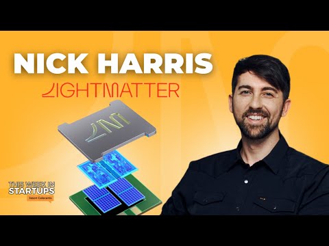 56:58
56:58Unlocking photonic computing with Lightmatter CEO Nick Harris
This Week in Startups · Interview
 24:44
24:44Is Photonic Computing The Future Of AI Chip Technology?
Forbes · Feature
 5:56
5:56What's next for photonics-powered data centers ft. Nick Harris
Sequoia Capital · Talk
 37:29
37:29Lightmatter InterConnect 2026 | The Future of AI Runs on Light
Lightmatter · Keynote
Founders

Nicholas Harris
Co-founder & CEO
MIT PhD in photonics who founded Lightmatter in 2017 to build light-based computing chips.

Darius Bunandar
Co-founder & Chief Scientist
MIT physicist and co-inventor of Lightmatter's photonic computing technology.

Thomas Graham
Co-founder
Co-founded Lightmatter out of MIT and led early business operations.